
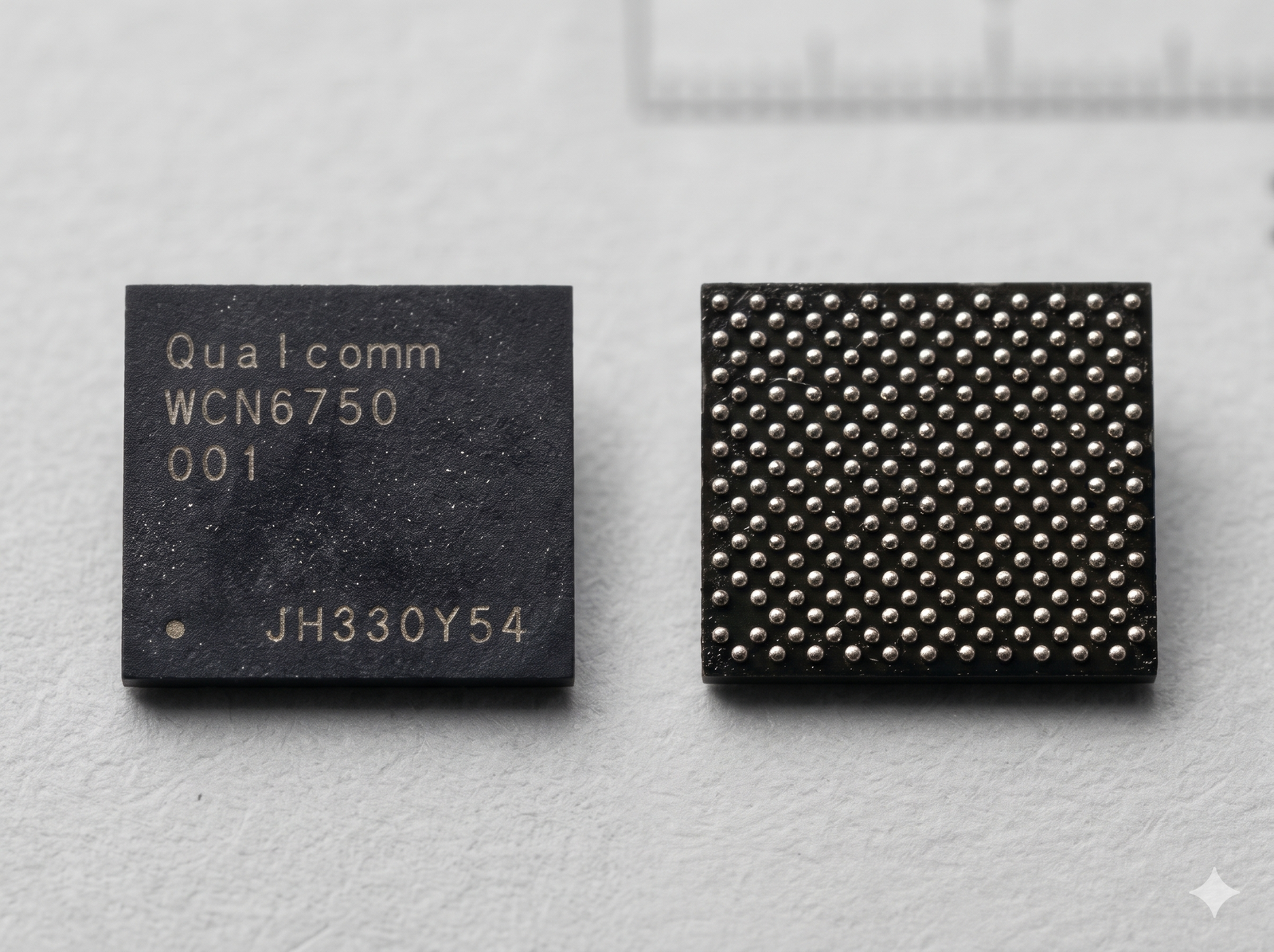
WCN6750 IC
Original Qualcomm WCN6750 (001) Wi-Fi 6/6E & Bluetooth 5.2 transceiver IC. Supplied in a pre-balled 14×12 BGA array with top-surface Pin 1 orientation indicator. Fully verified via Borneo Schematics across Samsung (A52s, A73, M52), Xiaomi/POCO (X5 Pro, Pad Pro, Mi 11/12 Lite), Realme (12/13 Pro+, GT Master), Vivo (V29, T1 Pro, Z6/Z7 Pro), Motorola Edge series, and Nothing Phone (1). Solves greyed-out Wi-Fi toggles, Bluetooth dropping, and motherboard short circuits.
₹220.00

Qualcomm WCN6750 IC
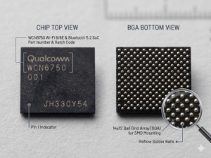
Qualcomm WCN6750 (001) Wi-Fi 6/6E & Bluetooth 5.2 IC
Short Description (Overview)
Original Qualcomm WCN6750 (001) Wi-Fi 6/6E & Bluetooth 5.2 transceiver IC. Supplied in a pre-balled 14×12 BGA array with top-surface Pin 1 orientation indicator. Fully verified via Borneo Schematics across Samsung (A52s, A73, M52), Xiaomi/POCO (X5 Pro, Pad Pro, Mi 11/12 Lite), Realme (12/13 Pro+, GT Master), Vivo (V29, T1 Pro, Z6/Z7 Pro), Motorola Edge series, and Nothing Phone (1). Solves greyed-out Wi-Fi toggles, Bluetooth dropping, and motherboard short circuits.
Product Overview & In-Depth Technical Description
The Qualcomm WCN6750 (Part Revision 001) is a monolithic, highly integrated wireless connectivity System-on-Chip (SoC) engineered specifically for mid-range and premium smartphone platforms. Manufactured on an ultra-compact footprint, this integrated circuit is dedicated to delivering next-generation Wi-Fi 6 / 6E and Bluetooth 5.2 capabilities directly to mobile motherboards.
In modern smartphone architecture, the WCN6750 operates in tandem with the primary Qualcomm Snapdragon application processor and PMIC power delivery lines. It manages dual-band and tri-band 2.4 GHz, 5 GHz, and 6 GHz RF transmissions, multiple input/multiple output (MIMO) processing, low-latency audio transmission, and Bluetooth LE operations.
Because connectivity chips process heavy continuous wireless data traffic and are positioned close to motherboard RF front-end modules, they endure significant thermal cycles, stress, and vulnerability to board flexion, drops, or liquid ingress. When physical drop shock or an electrical short on the VREG/LDO lines compromises this IC, replacing the component at the chip level becomes necessary to restore the device to complete factory operation.
This factory replacement IC comes in a 14 × 12 Ball Grid Array (BGA) configuration with factory-formed reflow solder balls, allowing direct SMD mounting on prepped PCB pads.
Common Faults & Diagnostic Symptoms It Resolves
A failing or physically cracked Qualcomm WCN6750 transceiver typically causes several distinct motherboard symptoms. Installing this replacement chip directly addresses:
-
Greyed-Out Wi-Fi Slider: The Wi-Fi toggle in phone settings is greyed out, disabled, or flips back to “Off” automatically immediately after toggling.
-
Bluetooth Inoperable / Searching Loop: Bluetooth fails to enable, shows an endless “Searching for devices” loop, or disconnects continuously during high-bitrate streaming.
-
Severe Signal Attenuation / Weak Range: Device only connects to a Wi-Fi router or Bluetooth device when placed directly against the antenna, caused by internal RF stage failure.
-
Motherboard Power Leakage & Heating: The area surrounding the Wi-Fi/BT shielding gets noticeably hot, accompanied by rapid battery drain even in standby mode.
-
Primary Line / Secondary Short Circuits: Dead phone condition or DC power supply reading high initial short/leakage (e.g., dead ground shorts on 1.8V VDD, 1.3V RF, or 0.9V core lines supplying the WCN6750).
-
System UI Freezing: Android OS temporarily freezes or stutters for 5–10 seconds every time Wi-Fi or Bluetooth auto-scan activates.
Hardware & Chip Package Specifications
-
Part Marking (Top View): Qualcomm WCN6750 001 with manufacturer batch code (e.g., JH330Y54)
-
Silicon Architecture: Qualcomm Wi-Fi 6/6E + Bluetooth 5.2 Mobile SoC
-
Package Mounting Style: Surface Mount Device (SMD) / BGA (Ball Grid Array)
-
BGA Grid Matrix: 14 × 12 Ball Array (168-pin footprint outline)
-
Ball Pre-balling: Factory pre-applied reflow micro solder balls
-
Orientation Feature: Distinct laser-etched circular dot on the top corner designating Pin 1 indicator
Complete Borneo Schematics Compatibility Matrix
Verified compatibility based on Borneo Schematics hardware database listings, cross-matching motherboards utilizing the Qualcomm WCN6750 series:
Brand / Manufacturer |
Supported Smartphone & Tablet Models |
Samsung |
• Galaxy A52s 5G (SM-A528 / SM-A528B) • Galaxy A73 5G (SM-A736 / SM-A736B) • Galaxy M52 5G (SM-M526 / SM-M526B) |
Xiaomi / POCO / Redmi |
• Mi 11 Lite 5G • Mi 12 Lite • Xiaomi Civi • Xiaomi Civi 2 • POCO X5 Pro 5G • POCO Pad (Wi-Fi Edition) • Redmi Pad Pro |
Vivo / iQOO |
• Vivo V29 • Vivo T1 Pro • iQOO Z6 Pro • iQOO Z7 |
Realme |
• Realme GT Master Edition • Realme 12 Pro+ (Pro Plus) • Realme 13 Pro • Realme 13 Pro+ (Pro Plus) • Realme P2 Pro |
Motorola |
• Moto Edge 20 (XT2143) • Moto Edge 2021 (XT2141) • Moto Edge 30 (XT2203) • Moto Edge 2024 (XT2405) • Moto Edge 50 (XT24xx) |
Nothing Phone |
• Nothing Phone (1) |
OPPO |
• OPPO Reno 10 Pro |
Huawei / Honor |
• Huawei P50 • Huawei Nova 9 • Huawei Nova 9 Pro • Huawei Nova 10 • Honor 50 • Honor 80 |
Micro-Soldering & Replacement Procedure for Technicians
-
Motherboard Preparation & Shield Removal:
-
Remove the logic board from the housing, disconnecting all cameras, display flexes, and batteries.
-
Apply high-temperature polyimide (Kapton) tape or thermal shield plates around surrounding processors, UFS memory chips, and neighboring sensors to shield against radiant heat.
-
Remove the RF shield can covering the Wi-Fi section using clean hot-air cutting or desoldering.
-
-
Faulty IC Removal:
-
Apply a generous amount of non-corrosive BGA rework flux around the edges of the defective WCN6750.
-
Using a micro-soldering hot air rework station with an appropriate nozzle, warm the board uniformly before concentrating heat over the IC at roughly 330°C–350°C (depending on airflow profile and lead-free board specifications).
-
Gently lift the IC using precision fine-tip tweezers once the solder has completely liquified. Avoid prying to prevent tearing PCB solder pads.
-
-
Pad Flattening & Conditioning:
-
Clean remaining solder from the PCB motherboard pads using desoldering wick/braid and a beveled soldering tip.
-
Ensure all pads are flat, shiny, and level. Clean with PCB cleaner or 99.9% isopropyl alcohol (IPA) and inspect under the microscope for missing or bridging pads.
-
-
Placement & Soldering:
-
Apply a thin, uniform film of tacky BGA flux onto the conditioned board pads.
-
Align the Pin 1 orientation dot on the top of the replacement IC with the PCB silkscreen indicator line.
-
Reflow with low-to-medium airflow until the chip gently floats and settles into position. A light tap with tweezer tips verifies surface tension alignment.
-
Allow the PCB to cool down completely before cleaning residue and reinstalling the RF shield.
-


Leave a Reply